Thursday, December 31, 2009

Some Layout Notes in avt2 RC2 20091230


I just uploaded layout notes on http://wiki.qi-hardware.com/wiki/Layout_notes_avt2_RC2_20091230
They are under http://wiki.qi-hardware.com/wiki/AVT2_RC2_Reference_Board#LAYOUT_NOTES, There are the layout histories about Qi's reference design board. We are the open team for everything on h/w platform. If you are interested with this open linux-based platform about consumer products, for example portable game player, mp3 player, dictionary, nano notebook or even like a high platform which can control Arduino board. Then you can use Qi's Ben NanoNote or its reference design board to reach variable applications. Check it if you want to follow hardware development, feedback welcome.

Tuesday, December 29, 2009

avt2 RC1 reference board


I just posted this specifications on Qi wiki page.
FEATURES
* 336 MHz XBurst Jz4720 MIPS­compatible CPU
* display: 8­bit RGB / ITU 656/601 data format input of TFT display.
* dimension (mm): 94.5 x 65
* DRAM: 64MB Synchronous DRAM
* headphone jack (3.5 mm)
* SDHC microSD
* support 850mAh charge limited 4.2V  Li­ion battery
* 2GB NAND flash memory
* mini­USB: USB 2.0 High­Speed Device
* micro­AB USB: USB 1.1 Host
* serial console
* speaker and microphone
* 58 Keys

Sunday, December 27, 2009

Jiaosi SieTian Temple, 宜蘭縣勅建礁溪協天廟

I'd like to know myself a little bit, so I went to SieTian Temple again to ask something that I firmly knew it about mine. After prayed, the aneswer is same as my thought. So i were happy and shocked beacuse all over the world that so many clinical diagnoses like me. Ok...then I think sometimes the ancient precepts who never cheat you. I must success then can post solutions in the future for those people like me. I will be like some sorts of asking patient to abstain from smoking. It won't too easy to do. But must to change and prove it.

Saturday, December 26, 2009

Friday, December 25, 2009

A Start on Wikipedia Syntax Learning


I am very happy that I can provide my contributions to http://wiki.qi-hardware.com/wiki/Special:Contributions/Adamwang, also including my blog here.

Learning something new is always a thanksgiving thing to someone. This is the job also interesting one. No one can block your idea or opinoin except unceasingly made a comment or criticism from others. Then learning or growing from overseas. It's real different from my previous Taiwanese job career type.

Thursday, December 24, 2009

My Pen Drive is dead

Shit! My pen driver is dead today. it shows that please format it. I didn't do that. So I tried to find any save disk program can survive it. Then I found it....that's the R-Studio

Tuesday, December 22, 2009

How to Record Skype Calls

Due to our meetings through skype..but my listening is not good.  so this recording tool can help me to practice english listening more...here's the tool.

Monday, December 21, 2009

Movenpick 莫凡彼冰淇淋


jeje...my friend bought me a lunch, almost like X'mas festival. Thanks my friend. The weather was so such ..cold today. This ice cream can let me felt the X'mas almost arrived now...this restaurant is came from Movenpick. I like this cute model.

Is there Any Open TV Platform in the Near Future


As title, is there any open hardware platform about TV even LCD display in the near future? I was thinking this couple months ago...now the answer is EXSITING.

Sunday, December 20, 2009

第53屆亞太影展勇奪最佳導演戴立忍的一席話


戴立忍:「痛心、憤怒、慚愧」:「我花了3年時間拍攝一部有關媒體自省的電影,沒想到3年功夫完全白費。」:「媒體最重要的應是保護未成年的當事者,沒想到部分媒體卻見獵心喜,不僅傷害了未成年的當事者與我的演員,也傷害了台灣。」:「我希望這部片能夠帶給台灣社會正面能量,如今卻因我的電影,傷害了兩個小朋友(真實事件中的女兒與飾演該角色的童星)。我拍這部片好像打開潘朵拉的盒子,看到了貪婪、本位主義、自私、不顧他人的立場,更看不到我片中所要講的『同理心』。」。「這是文明社會,某些隱私是不該拿出來講的,這是常識。」:「你還沒聽懂我的意思嗎?」
當我見這新聞時,我也想自己犯過同樣的錯誤,但若錯誤持續發生,這代表著甚麼涵意? 正如戴導演所言吧!!! 媒體從娛樂新聞的角色企圖搶得頭家的同時,卻失去客觀公正的報導倫理。我的生命過程中是否會存在著媒體的耳濡目染所影響,而能自律且能克服?各媒體人豈有萬般能耐可要求民眾盡能皆知?祇有時刻的提省自己。

推~~出類拔萃的新科亞太導演戴立忍~~支持你

我們不要這樣的媒體

時時被當頭棒喝的阿丹

Coffee

How's this coffee which is made by Mr. Brown Coffee? Actually it's quite not specially enough but beautiful one! Every bit is coming from creative idea if you have enthusiasm inside your heart, isn't it?

Saturday, December 19, 2009

What's Equivalent Circuit and Paramenters of Crystal


Many digital circuit it needs external crystal for microprocessor. And usually the datasheet tells you its input & output capacitance. So how you choose a Xtal's with correct parameters? The following descriptions can give you a formula.
Equivalent Circuit and Paramenters:

Equivalent Series Resistance ( R1 ):
The resistance is motional resistance ( series ) in the equivalent electric circuit. 
Motional inductance ( L1 ):
The inductance is the motional inductance ( series ) in the equivalent electric circuit.
Motional Capacitance ( C1 ):
The capacitance is the motional capacitance ( series ) in the equivalent electric circuit.
Shunt Capacitance ( Co ):
Shunt ( parallel ) capacitance ( Co ) is the capacitance between the crystal terminals. It is defference in package, usually it is less than 7.0pF.
Load Capacitance ( CL ):
The load capacitance is the circuit equivalent capacitance looking the circuit system from the two wire leads of crystal. The operation frequency in the circuit is defined by load capacitance and crystal.
U1 : ASIC
Y1: CRYSTAL
C1C2: capacitor which is connected
CL = [(C1*C2)/(C1+C2)] + Cstray CU1
Cstray : stray capacitance
CU1: IC’s input/output capacitance
Cstray and CU1 may varies from 2 to 6pF

A mobile life in the near future, as envisioned by NTT DOKOMO


How we can imagine that the near future of mobile life? The NTT DOKOMO is moving on...
http://www.nttdocomo.co.jp/english/corporate/future/hokusai/index.html
Those basical techs are :
a) e-paper
b)GPS/GPRS
c) 3.5G
d) 3D-interfaced
e) etc

so what they promoted couple of mature applications are as:
1) Vitual Museum & Advanced Search System
2) Simultaneous Interpreter Syttem
3) Virtual Edo
4) Hybrid Mobile Unit
5) Mobile Rehabilitation Robot
6) Nature Monitoring System
7) Mobile ID Security System
8) Automated Safety Drive System
Incredible!!! Better life is coming from big company...hope while they developing and still keep a wonderful and perfect earth's environment surrounding us....I think that i am / will feel it as well..

Wednesday, December 16, 2009

How to Solder RXD/TXD/GND in Ben NanoNote


This article is for Ben NanoNote's wiki page, you can also check here to know all the info in Qi Hardware's wiki page.

Purposes
    One wants to solder [1] extension wires for Ben NanoNote’s serial console test points. Since the Ben has that 3 test points (RXD, TXD & GND), it originally works as TEST POINTs on temporarily experimental or measurable purpose NOT permanently extendable one. Its original trace layout doesn’t allow you to do this under improper soldering method or carelessness. But if you still want to use serial port for a long while, this article can give you some guide lines.
Product
    Ben NanoNote
Tool & Material
    Soldering Station with a suitable conical type of soldering tip [2]
    Soldering Wire 0.5Φ diameter [3]
    Wire-Wrapping Wire 30AWG [4]
    Multi-function wire stripper [5]
Frequent Failures When Soldering
    Condition a, Test points ( Pads ) are broken from pcb surface
    Condition b, Trace with Test Point is pull out
Figure 1
    With improper soldering method or carelessness, you probably get either both or one of them.
Knowledge about Soldering
     Since the iron soldering tool can easily let you join two metallic surfaces into one, you need to be careful about your soldering head temperature, how many seconds you use and how about your craftsmanship you have. Before you start to do the following steps, you can also check the physical theory a little bit or ask anyone possessed of senior soldering skills to help you.
     Through [1], you can see more soldering articles for your reference. Also you can check here [7] to know HOW TO SOLDER first.
STEPs
A . Soldering Accessories
     A 900M-T-1 size of soldering iron tip can be suitable for this process. You can choose a 1 or 3 marked tip as following figure. The marked 2 or 4 is not recommended.

Figure 2
Figure 3
    A 0.5mm diameter soldering wire is better.
Figure 4
    Also using a 30AWG of wire wrapping wire or equivalent AWG wire is recommended.
Figure 5
    Why choose so tiny diameter accessories? Please see next figure then you will easily realize. Unless you are an expertise with great craftsmanship in soldering field, I do really recommend that using them.
Figure 6
B. CLEAN up test points and wires
 The TXD (TP75) and RXD (TP74) are shown as below. Or see [8] [9] to understand their location. Clean up the surface of test point and wires first, you can just follow “ 2. SURFACE PREPARATION: CLEAN” instructions of [7] to do this step. Novices can make the mistake of overheating the parts as they try to force the solder to stick. This will usually result in irreversible damage and force you to scrap pads, trace or even BEN Nanonote.
                                               Figure 7                                          Figure 8
C. Tinning
     Contacts of both test points and wires must be tinned before attempt to solder. So now do tinning process on 3 test points and terminal of three wires as next figure as well. Some wire wrapping wire already have been tinned on its surface, you can just use a wire stripper to strip away the tip of the insulation to expose the copper wire within. Otherwise you must lightly coat it with solder. You must also tin the tip of the iron to help conduct heat to the components.
Figure 9
D. Applying Heat and Solder
     Before doing this step of real solder you can reference this video [10] to see how solder will be the better. “With the tinned soldering iron in hand, you are now ready to heat the components. Rest the iron tip on both the wire lead and the PCB. It will only take one or two seconds to heat the components up. Once you have heated up the wire and the circuit board, solder can be applied. Touch the tip of the strand of solder to the heated wire lead and the solder pad on the circuit board, but not to the tip of the iron. At this point, the solder will flow freely around the wire lead and the pad. Once the surface of the pad has been completely coated, you must stop adding solder and then, quickly remove the soldering iron. Do not move the newly formed joint for a few seconds until the solder cools down and becomes solid. Moving the joint at this point will cause a formation of a cold joint.”
Figure 10
E. Clean up
    Clean up again on all soldered area.
F. Fixed by glue or other adhesive tape
     Using any adhesive tape or glue is to protect wire-wrapping wires away from heavy extra-loading forced to bend wires, pull out test points or break trace shown as figure 1. If you’d prefer to use usb power rather than battery, you can just do like as following figure or use adhesive tape to protect those three soldered point.
Figure 11
Ref.
[1] http://en.wikipedia.org/wiki/Soldering
[2] http://www.sparkfun.com/commerce/product_info.php?products_id=619
[3] http://www.senju.com/pages/lead_free_wire.htm
[4] http://cgi.ebay.com/_W0QQcmdZViewItemQQitemZ120478983749
[5] http://www.sparkfun.com/commerce/product_info.php?products_id=8696
[6] http://www.tequipment.net/HakkoCSP30-1.html
[7] http://www.solderinguide.com/
[8] http://wiki.qi-hardware.com/wiki/Serial_console
[9] http://wiki.qi-hardware.com/wiki/File:Ben_nanonote_serial2.jpg
[10] http://vega.org.uk/video/programme/166
 Author: adam@qi-hardware.com

Monday, December 14, 2009

Experiment of Ben NanoNote's Charge Cycle


I just edited this at Qi Hardware wiki. So you can also see this article here.

Purpose of Experiment 
    To understand that how does Ben NanoNote’s charge cycle work.

Test Product
    BEN NanoNote

Equipments
    Agilent 34401A Multimeter
    CHY 48R Multimeter

Methods of Connection
    Current connection:

Figure 1
Schematic
Figure 2
State Diagram of a Typical Charge Cycle
Figure 3
Study System Voltage Specification
Before this experiment, let’s see how Ben’s design and how to choose low voltage detector first. Because the Ben has jz4720 VDDIO voltage (2.97~3.63V) see page 24 of datasheet [1], the NANAD FLASH K9GAG08U0M has Vcc range (2.7~3.6V), also SDRAM P3V56S40ETP has VDD range (3.0~3.6V). So a low voltage detector circuit that can shut down the cpu jz4720 when monitors Battery’s voltage goes down -VDET (2.94~3.06V) detected by BL8506-30NRM, and the Battery has a over-discharge protect voltage 2.25V.
Figure 4

Through figure 4, we can easily know the best working power voltage for ben should be between upper limited 3.6V of SDRAM and lower limited 3.0V of SDRAM. That’s their intersection. Of course if there’s an sdram with widely working voltage like nand flash at lower 2.7V. That would be good to lengthen discharging time. But then the intersection becomes 2.97V caused by cpu. Since battery cell has overdischarge protect voltage 2.25V, strongly recommended that the software should be possessed of a detector of monitoring battery voltage under 3.0 voltages to make sure sdram can work normally. That’s the reason why ben has a low voltage detector BL8506-30NRM [3] which is based on 3.0±0.06 V detection precision ±2%.

Charge Status Indicator (CHRG), pin1 of SE9016
From its datasheet [2], this pin can output three status: strong pull down(~ 10mA), weak pull down (~20uA) and high impedance. So D3 LED can be as indicator shown if charging or not.

Experimental Data
From SE9016 datasheet [2], when BEN is on Power ON mode (Display On) , PW_ON_N is low; so RPROG = R15 = 10KΩ, from Data collection, IBAT = (VPROG / RPROG ) * 1100, then we can calculate VPROG inversely from measured IBAT.
Before measurement, make sure that the battery is above 3.06V, otherwise the low voltage detects will tell s/w to shut down cpu and will enter POWER OFF mode. This experiment will split into two modes to measure different charge current.

Case a: POWER ON mode, PW_ON_N is low, Display ON, Slow charging
Case b: POWR OFF mode, PW_ON_N is high, Display OFF, Fast charging
We firstly let BEN entered into POWER ON mode to keep the RPROG equaled to 10KΩ, not 2 KΩ. (if enters POWER OFF mode, the high PW_ON_N will let Q3 TM2302FN turned on then RPROG is R14//R15. see figure 2). From the measured data [4] or figure 5 and 6. The data is a result that starts from 3.6V battery and charges it until ascending theoretically preset 4.2V charge voltage with ±1% accuracy thus 4.158V. Experimentally a 4.145V measured. When the bat pin approaches the final float voltage (4.2V), the SE9016 enters constant-voltage mode and the charge current begins to decrease. We can realize it needs 16.8 hrs from 3.6V to 4.2V.

Figure 5
Figure 6

There’s a voltage called “overdischarge protect/preventing voltage” for lithium-based battery. After measured Ben’s descendant voltage during its discharging, a 2.3V measured then battery inside turn off its output voltage to 0V. This is within its specification 2.25~2.35V. So can let Ben’s SE9016 acted as following figure.
Figure 7
Once VBAT > 2.8V and VPROG > 100mV, SE9016 charges as next figure which is stated in CC/CV mode.
Figure 8
Now let Ben entered to POWER OFF mode to keep the RPROG equaled to 2 KΩ. (R14//R15. see figure 2). From the measured data [4] or figure 9 and 10. The data is a result that starts from 3.2V battery and charges it until ascending preset 4.2V charge voltage with ±1% accuracy thus 4.158V. Experimentally a 4.135V measured. It needs 2.68 hrs from 3.2V to 4.135V. Afterwards, SE9016 enters constant-voltage (CV) mode and the current begins to decrease. The plot of figure 7 & 8 doesn’t include data of CV mode.
Figure 9


Figure 10
The standby mode of SE9016 didn’t experiment. Also see figure 8 in blue flow. To manually restart a charge cycle when in standby mode, the input voltage ( usb power ) must be removed and reapplied or the charger must be shut down and restarted using the PROG pin.

This result of experiment may be based on unique battery applied and referenced. You can also find this standard battery technology in many other devices. Ben batteries share the characteristics common to lithium-based technology in other devices. Like other rechargeable batteries, these batteries may eventually require replacement.

[1]http://downloads.qi-hardware.com/hardware/qi_avt2/v1.0/datasheet/U1~Jz4720_ds.pdf
[2]http://downloads.qi-hardware.com/hardware/qi_avt2/v1.0/datasheet/U5~SE9016.pdf
[3]http://downloads.qi-hardware.com/hardware/qi_avt2/v1.0/datasheet/U7~BL8506-30NRM.pdf
[4]http://downloads.qi-hardware.com/hardware/qi_lb60/report/charge_cycle/data.ods
[5]http://www.mpoweruk.com/chargers.htm#rates
[6]鋰電池的守護神---鋰電池保護IC的重要性

Author: mailto:adam@qi-hardware.com

Sunday, December 13, 2009

Guns N Roses - Chinese Demoncracy World Tour - Taipei Concert


Be an endless paradise heart inside of mine.... endless fan i am....no matter whoever around the world critizes him or not......he's AXL.....who cares.....when you really realiy to be a fan to him ....no matter what age he is/will...fatter/thinner....that's him...
I watched tons of clips in Youtube....If you love him...you'll love him forever....me too
because that has already been my part of life during teenage. I sincerely cherish it.
I think that I won't forget this 2009/12/11 in my life, Guns N Roses concert tour of Asia's first station dedicated to the Taipei Taiwan. I like a few tens of tune, there appeared such as Chinese DemacracyKnocking on Heaven's DoorNovermber Rain which this time he played piano by himself too. Actually he sang twice "December" Rain.....jeje...I liked it. because it was really rainning at that time. Welcom to the JungleSweet Child O' MineParadise City, in particular, although I watch away games, the audience sang along with the beat beat time to sing Knocking On Haven's Door, I was almost came out of tears around eye's corners. After say good bye, Guns N Rose continued to open singing, the audience wild. I was no exception. like it, there is no great truths, even if he appeared an hour later! So what ! That's him, and he is still the same as before I like. 
  
Here is the setlist for this show:

1. Chinese Democracy
2. Welcome To The Jungle
3. It's So Easy
4. Mr. Brownstone
5. If The World
6. Live And Let Die *Richard Fortus Solo (James Bond Theme)
7. There Was A Time *Frank Ferrer Drum Solo *Tommy Stinson Bass Solo
8. My Generation (Stinson vocals)
9. I.R.S.
10. Rocket Queen *Dizzy Reed Piano Solo
11. Street Of Dreams *DJ Ashba Solo
12. Sweet Child O' Mine *Band Jam
13. November Rain *Ron Thal Solo (Pink Panther)
14. You Could Be Mine
15. Shackler's Revenge
16. Knockin' On Heaven's Door

**--- ENCORE ---**

17. This I Love *Band Jam
18. Better
19. Paradise City

Look at my achievement from shopping! I bought T-Shirt and a hat. I am loving it. A close look at the back of my shirt Oh!!?? is the Asian tour of the country location, had the opportunity to visit the first tour station in Taipei of it's concert. If you want to know about them, you can go to www.gunsnroses.com 
 

Wednesday, December 9, 2009

Taiwan Panorama Magazine

I'd like to introduce a magazine that I love to read it so much, especially as long as I have time then I read article from them, then I really feel better after reflashed my brain. It's the Taiwan Panorama Magazine, i first read it during my senior high school. Even I've been subscribed a year at that time. Until now I still subscribe it but in the internet. I was attracted to its beautiful translation, in particular, it is in caring for all of Taiwan's bit by bit. Through it, you will learn even more profound about Taiwanese culture. Hope you can enjoy.

Tuesday, December 8, 2009

Selling avt2 board from Qi Hardware Inc.


If you like linux world, also includes Ingenic jz4720 CPU, USB host/device, 64MB SDRAM, 2GB Flash with serial console connector which can let you access to and from laptop, then you can buy this avt2 reference board.

You can get all open sources here:
software
hardware, schematic, pcb files, gerber files

Having this avt2 board, you can participate with the development of Qi Hardware Inc. next product.

Monday, December 7, 2009

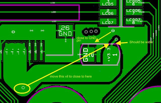
How to Playcement and Layout Bypass Capacitor Sequencing with Vils


Bypass Capacitor is used to bypass the power supply or other high impedance component of a circuit. I found that any through vils applied in board design, you must to know what the signal you want to let it pass through and what signals you want to eliminate as more as possible. For example, there's a capacitor needed placement as close as LCD FPC connector with 10uF/10V. but how you route the trace on board?
 The above placements of vils are not perfect. You can see the descriptions of bypass capacitor first.Then you can check Parasitic Inductance of Bypass Capacitor II to know what's relationship between your vils with your bypass capacitor? and how's the parasitic inductance of bypass capacitor?

Putting aside the very basics of the theory, let us use the simplest principles of the road point of view, in the end the diameter of vil how we choose? First of all, if one has a four-lane highway through the lane, and then an A at suddenly reduced to two lanes of carriageway; but through the B Division turned back after the four-lane carriageway, what will it happen? A result, will be have traffic jam phenomenon before entering the A, but once through A then becomes smooth into two lanes. After a B point, the phenomenon of traffic congestion would not occur again. 

Back to the original topic, if the bypass capacitor connected to vil which its circumference range as long as alike AB, and then also if the original trace width and following trace width is inconsistent, there will be unintended consequences.
 
If track width is 0.0118", then the both terminal side of each wire trace, the vils should bigger than track width;
for example:
        track width = 0.0315", 
        through vil's diameter = 0.0118"
        then the length of the circumference (c) = 2 * 3.141592 * ( 0.0118 / 2 ) = 0.037"
since we are not sure normally the quality on processing vils on pcb maker, so the most safe way is to put
2 pcs of 0.0118" through vil (total equivalent width = 0.037 * 2 = 0.074) on the two ends of trace.

From above illustration, you can see either 2πis shorter than layer 1 trace width or layer 2 trace width, you will have a wrong choose on vil width type or amount of vils.

Let's go back a little bit of theory side, please reference to this in advance. Through it, in general, if you want to have an overall quick view, you can watch its Index by Keyword for your like hand book.

To be continued.
Ref. : PCB LAYOUT AUTHORITY

Thursday, December 3, 2009

Qi Hardware Inc. has Kicad version reference design

Qi Hardware Inc. just finished pcb and gerber files used by Kicad free tool, i am double checking these great results. You can see here to know all of them.

Ben Nanonote Taking Fun with Games

It's really great news that Ben Nanonote now can play games, you can see here, thanks to David & XiangFu. In the future, maybe Ben Nanonote can be as a portable game player once wifi module runs stable. You can also go to official site here to see it.

Wednesday, December 2, 2009

charging questions on ben nanonote


i sent an email to list for asking following questions, also you can see the following reply messages here.
------------------------------------------------------------------------------------------------------------------------------------
When I measured Ben's charging circuit, I have some questions for s/w hacker:

a) how kernel know that the battery charging if done or in charing?
     Using ADIN0 (pin 92) of jz4720 to check voltage of VBAT? this pin is directly connected to battery cell.
     If you use this to judge, how you manage s/w to shut down ben when battery's voltage goes down under 2.94V?
     you can see [1] &[2], to know SHUTDOWN (GPD6) can tell cpu when components U7 [3] found there's a low voltage detected,
     so means that you may need to do something on software to do store & save tasks then turn off device.

b) has anyone used net name called "CHARGE_N" thus GPC27 (pin 69) of jz4720?
    what status did you initial this pin? input or output? have any help to you?
    Why I asked these questions? Please see [4],
ch1 = CHARGE_N / GPC27 of jz4720
 ch2 = pin 1 of U5 SE9016
I am thinking that using this "CHARGE_N" pin(GPC27) [5] as input then you can let cpu known the status if charging is done or not by h/w, not judge only by ADIN0; so then maybe you can code an icon at UI to let user know that the device is at usb charging mode or battery mode.
Sorry I don't know s/w side. Thanks a lot.
Adam

[1] http://downloads.qi-hardware.com/hardware/qi_avt2/v1.0/report/waveforms/lb60/lb60_12.jpg
[2] http://downloads.qi-hardware.com/hardware/qi_avt2/v1.0/report/waveforms/lb60/lb60_waveform_description
[3] http://downloads.qi-hardware.com/hardware/qi_avt2/v1.0/datasheet/U7~BL8506-30NRM.pdf
[4] http://downloads.qi-hardware.com/hardware/qi_avt2/v1.0/report/waveforms/lb60/lb60_3.jpg
[5] http://wiki.qi-hardware.com/wiki/Power_Supply_Circuit

Tuesday, December 1, 2009

Easy Book 上網通GL-740

最近有人傳這個Easy Book 上網通GL-740 資訊給我, 其實我在 Shenzhen 時已經看到很多這類產品; 大陸都稱它為"上網本"; 超輕的, 只有 0.68Kg; 跟 Qi Hardware Inc. 的產品有類似喔!!! 但  Qi Hardware 的 Ben Nanonote 是要外掛 MicroSD wifi module 才可上網, 但都是用  Ingenic 的 CPU.

Some waveforms about Ben Nanonote of Qi Hardware Inc.


I just curious on Ben Nanonote h/w, so I took some waveforms on its board. For much understanding that h/w behaviour, so collected some waveforms about Ben Nanonote and avt2 reference board. You can refer to here [1] to know. Since the avt2 board [2] is the reference developed from with Ben, you can directly check [3] for your reference, taking them you may easily understand how Ben works like power on or off sequences.

[1] http://downloads.qi-hardware.com/hardware/qi_avt2/v1.0/report/waveforms/
[2] http://downloads.qi-hardware.com/hardware/qi_avt2/v1.0/report/waveforms/avt2/avt2_waveform_description
[3] http://downloads.qi-hardware.com/hardware/qi_avt2/v1.0/report/waveforms/lb60/lb60_waveform_description

Gold Phoenix PCB Co.,Ltd


I found another new pcb maker called Gold Phoenix PCB Co.,Ltd.
I hopefully can contact with this vendor which is located near the Wuhan Dong Hui Industry Zone.