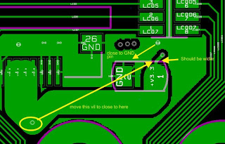
Bypass Capacitor is used to bypass the power supply or other high impedance component of a circuit. I found that any through vils applied in board design, you must to know what the signal you want to let it pass through and what signals you want to eliminate as more as possible. For example, there's a capacitor needed placement as close as LCD FPC connector with 10uF/10V. but how you route the trace on board?
The above placements of vils are not perfect. You can see the descriptions of bypass capacitor first.Then you can check Parasitic Inductance of Bypass Capacitor II to know what's relationship between your vils with your bypass capacitor? and how's the parasitic inductance of bypass capacitor?
Putting aside the very basics of the theory, let us use the simplest principles of the road point of view, in the end the diameter of vil how we choose? First of all, if one has a four-lane highway through the lane, and then an A at suddenly reduced to two lanes of carriageway; but through the B Division turned back after the four-lane carriageway, what will it happen? A result, will be have traffic jam phenomenon before entering the A, but once through A then becomes smooth into two lanes. After a B point, the phenomenon of traffic congestion would not occur again.
Back to the original topic, if the bypass capacitor connected to vil which its circumference range as long as alike AB, and then also if the original trace width and following trace width is inconsistent, there will be unintended consequences.
If track width is 0.0118", then the both terminal side of each wire trace, the vils should bigger than track width;
for example:
        track width = 0.0315",
        through vil's diameter = 0.0118"
        then the length of the circumference (c) = 2 * 3.141592 * ( 0.0118 / 2 ) = 0.037"
since we are not sure normally the quality on processing vils on pcb maker, so the most safe way is to put
2 pcs of 0.0118" through vil (total equivalent width = 0.037 * 2 = 0.074) on the two ends of trace.
From above illustration, you can see either 2πr is shorter than layer 1 trace width or layer 2 trace width, you will have a wrong choose on vil width type or amount of vils.
Let's go back a little bit of theory side, please reference to this in advance. Through it, in general, if you want to have an overall quick view, you can watch its Index by Keyword for your like hand book.
To be continued.
Ref. : PCB LAYOUT AUTHORITY
Let's go back a little bit of theory side, please reference to this in advance. Through it, in general, if you want to have an overall quick view, you can watch its Index by Keyword for your like hand book.
To be continued.
Ref. : PCB LAYOUT AUTHORITY


No comments:
Post a Comment